Traditional optical chipmaking lenses become completely opaque to deep ultraviolet wavelengths; Hiroo Kinoshita carved microchip circuits using extreme ultraviolet soft X-rays reflected off atomic-precision multilayer mirrors. Published in 1989 when the industry deemed X-ray lithography an impossible fantasy, Kinoshita’s experimental setup became the physical foundation of the multi-billion-dollar ASML EUV machines that print the world's most advanced computer chips.
In semiconductor fabrication, printing smaller transistors requires shining light with smaller wavelengths through glass lenses. However, as wavelengths approached extreme ultraviolet, a physical wall was hit: glass lenses absorbed the light like concrete, making traditional camera optics useless.
Japanese physicist Hiroo Kinoshita realized that instead of shining light through glass lenses, chipmakers had to bounce soft X-rays off ultra-smooth atomic mirrors in a total vacuum. By coating mirrors with alternating layers of molybdenum and silicon, his team created an atomic telescope capable of focusing 13.5-nanometer light onto silicon.
Dormant for three decades while the industry stretched immersion lithography to its limits, Kinoshita's mirror design now powers the global microchip supply chain. By printing the world's fastest two-nanometer AI processors, by enabling ASML’s $300-million lithography machines, and by driving global technology geopolitics, EUV mirror physics shapes human civilization.
Soft x-ray reduction lithography using multilayer mirrors
A soft x-ray lithograpy using multilayer mirrors for demagnifying optics and a reflecting mask has been designed and studied experimentally. In this system, a wavelength of 45–130 Å has been selected based on the optical characteristics, the exposed depth of the resist film, and the reflectivity of the multilayer mirror. To obtain a replication pattern resolution of 0.2 μm, the numerical aperture required is estimated to be greater than 0.0125 or 0.0325 for a wavelength of 50 or 130 Å, respectively. These values show that the multilayer optics using two mirrors can be realized to replicate a 0.2 μm pattern. The experiments were performed on the SR beamline BL-1 of the KEK-PF storage ring. The Schwarzschild demagnifying optics with a ring field were designed and fabricated. Demagnified exposure patterns of less than 0.5 μm have been obtained using a reflecting mask. The feasibility of the soft x-ray reduction method using multilayer mirrors has been confirmed. Furthermore, new telecentric optics are proposed to realize a practical reduction lithography system.


Physicists universally believed that the laws of nature look completely identical when viewed in a mirror; Chien-Shiung Wu proved that radioactive atoms preferentially shoot electrons in only one direction, proving that nature has an intrinsic left-handed bias. Executed at cryogenic temperatures in 1957, the "Wu Experiment" shattered the sacred law of Parity Conservation, revolutionizing particle physics and laying the foundation for the electroweak Standard Model.


Most fast-conducting solid electrolytes corrode into useless sludge when they touch pure metallic lithium; garnet-type ceramic crystals conduct lithium ions rapidly while remaining completely impervious to corrosive lithium metal. Discovered in 2003 by Thangadurai and Weppner, this sleeping beauty crystal is now the foundational solid electrolyte behind multi-billion-dollar solid-state battery startups like QuantumScape.
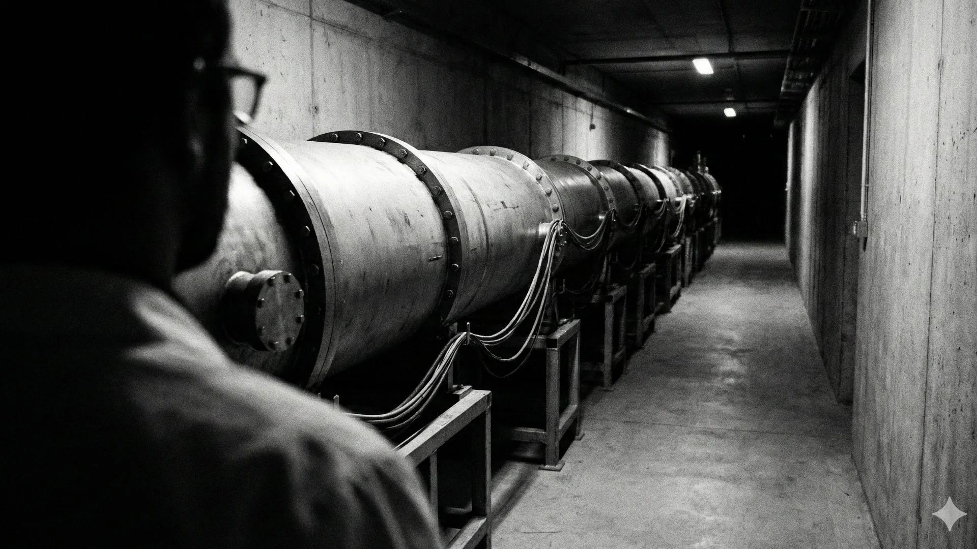

Direct dark matter detection experiments were historically deaf to low-mass particle interactions; XENON1T's ultra-pure liquid xenon time projection chamber uncovered a tantalizing excess of low-energy electronic recoils deep beneath an Italian mountain.

First-order cosmological phase transitions in the early universe expand as seething vacuum bubbles whose speed determines gravitational wave signatures; first-principles hydrodynamic calculations establish exact bubble wall velocity benchmarks without phenomenological friction.

The James Webb Space Telescope stunned astronomers by discovering thousands of mysterious glowing red dots that appeared to be impossibly massive galaxies formed right after the Big Bang; deep infrared imaging proved that these dots are dense cosmic cocoons where baby supermassive black holes are rapidly devouring gas. Published in The Astrophysical Journal, this discovery solves JWST’s "Little Red Dot" mystery, explaining how giant supermassive black holes grew in the early universe without breaking cosmological laws.


Telecommunication engineers believed that static noise permanently corrupted electrical signals; Claude Shannon proved that information can be transmitted with zero errors across noisy channels by converting meaning into binary bits. Published in 1948, Shannon’s masterwork founded information theory and created the digital language of the modern world.


People assumed that close friends and family members were the most important allies for finding a new job and getting ahead in life; Mark Granovetter proved that casual acquaintances you barely talk to are the single most valuable source of new career opportunities and fresh ideas. Published in 1973, "The Strength of Weak Ties" is one of the most influential sociology papers in history, providing the network blueprint that built LinkedIn and modern professional networking.


Physical sensors in rockets and satellites are constantly corrupted by noise, vibration, and sensor drift; Rudolf Kalman developed an optimal mathematical filter that predicts true position by fusing imperfect sensor readings with equations of motion in real time. Published in 1960, the Kalman Filter guided the Apollo spacecraft to the Moon and is the mathematical brain powering every GPS receiver, autonomous drone, and commercial jetliner on Earth.
Ask this paper your own questions, or keep browsing the verified research catalogue.